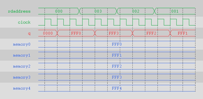
The following waveforms show the behavior of altsyncram megafunction for the chosen set of parameters in design ram_2p_ils.vhd. For the purpose of this simulation, the contents of the memory at the start of the sample waveforms is assumed to be ( FFF0, FFF1, FFF2, FFF3, ...). The design ram_2p_ils.vhd has one read port and one write port. The read port has 1024 words of 16 bits each and the write port has 1024 words of 16 bits each. The ram block type of the design is M4K. The output of the read port is registered by clock.
The above waveform shows the behavior of the design under normal read conditions. The read happens at the rising edge of the enabled clock cycle. The output from the RAM is undefined until after the first rising edge of the read clock.
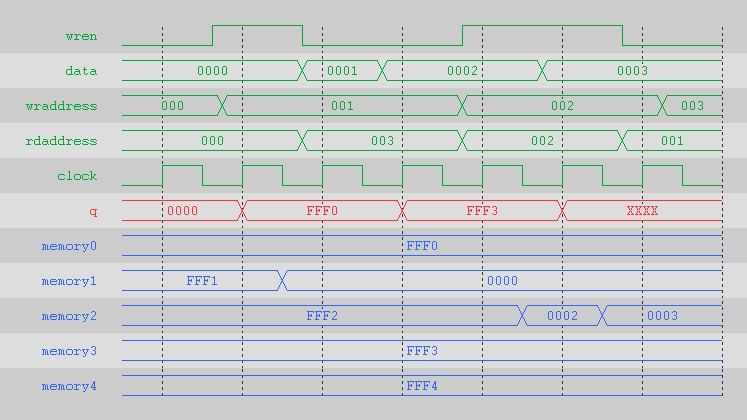
The above waveform shows the behavior of the design under normal write conditions. The write cycle is assumed to be from the rising edge of the enabled clock in which wren is high till the rising edge of the next clock cycle. In DUAL_PORT mode, when the write happens at the same address as the one being read in the other port, the read output is unknown. Actual write into the RAM happens at the falling edge of the write clock.