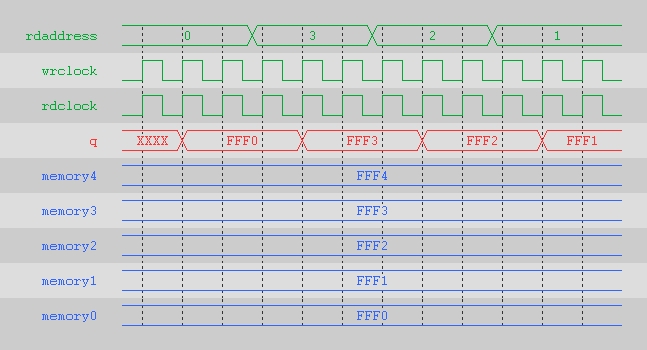
The following waveforms show the behavior of altsyncram megafunction for the chosen set of parameters in design ni_dpram.vhd . For the purpose of this simulation, the contents of the memory at the start of the sample waveforms is assumed to be ( FFF0, FFF1, FFF2, FFF3, FFF4, ...). The design ni_dpram.vhd has one read port and one write port. The read port has 2048 words of 16 bits each and the write port has 4096 words of 8 bits each. The ram block type of the design is AUTO . The output of the read port is registered by rdclock.
The above waveform shows the behavior of the design under normal read conditions. The read happens at the rising edge of the enabled clock cycle. The output from the RAM is undefined until after the first rising edge of the read clock.
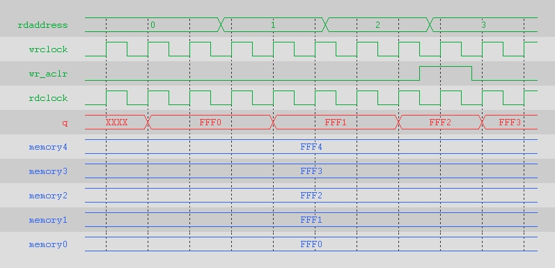
The above waveform shows the behavior of the design under read conditions with clears on input and/or output registers. The read happens at the rising edge of the enabled clock cycle. The read cycle is assumed to be from the rising edge of the clock cycle till the next rising clock edge.
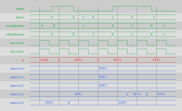
The above waveform shows the behavior of the design under normal write conditions. The write cycle is assumed to be from the rising edge of the enabled clock in which wren is high till the rising edge of the next clock cycle. In DUAL_PORT mode, when the write happens at the same address as the one being read in the other port, the read output is unknown. Actual write into the RAM happens at the rising edge or falling edge of the write clock, depending on whether the RAM blocks are assigned to M-RAM or not. In the sample waveforms, they are shown to be on the falling edge of the write clock.
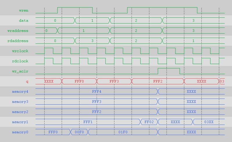
The above waveform shows the behavior of the design under write conditions with clear(s). A clear on the write address during a write cycle corrupts the whole RAM (The contents of the RAM become unknown). A clear on the input data during a write cycle corrupts the RAM contents in that particular address (The contents become unknown). A clear on the write enable during a write cycle corrupts the RAM contents in that particular address (The contents become unknown).